 ASVAB Camp

Learning goals and EI scope
After this lesson you should be able to explain what makes silicon a semiconductor and how doping creates n-type and p-type material. You should describe a P–N junction and predict when a diode conducts or blocks.
You should also recognize LEDs, photodiodes, and Zener diodes by function, explain how BJTs and MOSFETs act as switches, and work idealized problems on LED resistors, diode power, Zener current, and transistor gain using the values a question supplies.
Why semiconductors matter in EI
Almost every modern electronic product depends on semiconductor devices. The phone in your pocket, the radio in a vehicle, a radar display, and the charger for a battery pack all contain diodes, transistors, and integrated circuits made from semiconductor material.
The ASVAB Electronics Information test does not expect you to design chips. It expects you to know what these devices do: which one passes current one way, which one gives off light, which one senses light, which one switches or amplifies, and how to work a few basic numbers. Knowing the purpose of each device lets you reason through questions even when the wording is unfamiliar.
Distinguish conductor, insulator, and semiconductor
Materials fall into three broad groups by how easily they carry current. Conductors, such as copper, aluminum, and silver, have many free electrons and carry current easily. Insulators, such as rubber, glass, and dry wood, have almost no free charge carriers and block current under normal conditions.
Semiconductors, such as silicon and germanium, sit between those extremes. Pure silicon conducts poorly at room temperature, but its conductivity can be raised greatly and precisely by adding small amounts of other elements, or by heat or light. That controllability is exactly why semiconductors are useful: engineers can design where and how current flows.
Silicon and its crystal structure
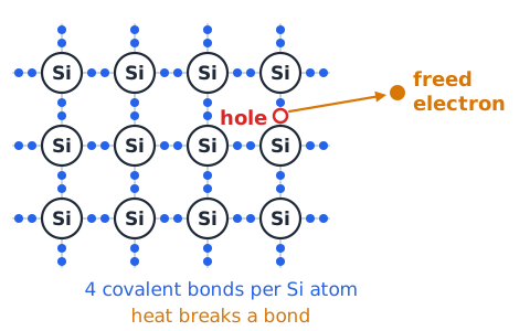
Silicon is the most widely used semiconductor. It is made from ordinary sand (silicon dioxide) refined to extremely high purity. Each silicon atom has four outer, or valence, electrons.
In a silicon crystal, every atom shares one electron with each of four neighbors, forming four covalent bonds in a regular three-dimensional pattern called a lattice. Because those electrons are tied up in bonds, very few are free to move, so pure silicon is a weak conductor. Heat can knock a few electrons loose. Each freed electron leaves behind an empty spot in a bond, called a hole, which can also help carry current.
Energy bands without unnecessary quantum math
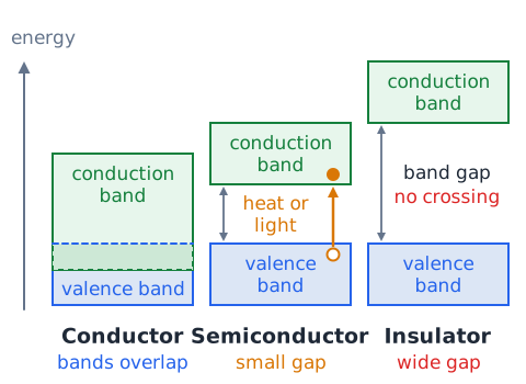
A simple picture helps explain why materials differ. Electrons in a solid can only have energies within certain ranges called bands. Electrons in the lower valence band are held in bonds. Electrons that reach the higher conduction band are free to move and carry current.
The space between the two bands is the band gap. Conductors have overlapping bands, so electrons move freely. Insulators have a wide gap that electrons almost never cross. Semiconductors have a small gap, so some electrons jump across with heat or light energy. You do not need equations for the ASVAB, only this ranking of gap size.
Doping means a controlled impurity
Doping is the deliberate addition of a tiny, carefully measured amount of another element, called an impurity or dopant, to pure silicon. Even a few dopant atoms per million silicon atoms can raise conductivity by a huge factor.
The dopant atoms take the place of silicon atoms in the crystal. Depending on how many valence electrons the dopant has, it either supplies extra free electrons or creates extra holes. Doping does not change silicon into a different element or change the mass of electrons. It changes how many charge carriers are available, and therefore how well the material conducts.
N-type material: electron majority carriers
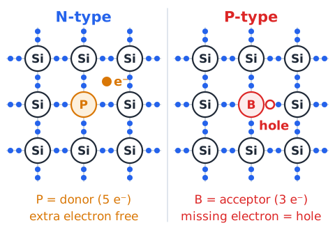
N-type silicon is made by adding a dopant with five valence electrons, such as phosphorus, arsenic, or antimony. Four of those electrons bond with neighboring silicon atoms, and the fifth is only loosely held. It easily breaks free and moves through the crystal.
Because these dopants donate electrons, they are called donors. In n-type material, free electrons are the majority carriers, and the few holes created by heat are the minority carriers. The "n" stands for negative, since the main mobile carriers are negatively charged electrons. Current in n-type material is carried mostly by electron motion.
P-type material: hole majority carriers
P-type silicon is made by adding a dopant with three valence electrons, such as boron, gallium, or aluminum. The dopant can form only three complete bonds, leaving one bond short an electron. That gap is a hole.
A nearby electron can hop into the hole, which leaves a new hole where it came from. The hole appears to move, and it behaves like a positive carrier. Because these dopants accept electrons, they are called acceptors. In p-type material, holes are the majority carriers and free electrons are the minority carriers. The "p" stands for the positive behavior of holes.
Majority carriers are not total charge
A common mistake is to think that n-type silicon is negatively charged and p-type silicon is positively charged. Both are electrically neutral overall.
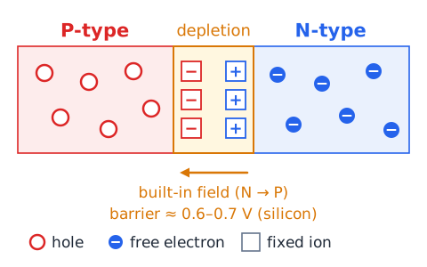
Each donor atom that releases a free electron is left as a fixed positive ion, so the extra electron and the ion balance. Each acceptor atom that captures an electron becomes a fixed negative ion, balancing the hole. The labels n and p describe which mobile carrier dominates, not the net charge of the whole piece. Only where two regions meet, at a junction, do separated charges create a local electric field.
What a P–N junction is
A P–N junction is formed when p-type and n-type regions are created next to each other in one continuous crystal. It is not two pieces simply pressed together.
At the boundary, free electrons from the n side diffuse into the p side and fill holes, and holes diffuse the other way. This leaves a thin zone near the boundary with almost no mobile carriers, called the depletion region. The fixed ions left there create an electric field and a built-in voltage, roughly 0.6 to 0.7 V for silicon. That barrier is what gives a diode its one-way behavior.
Equilibrium does not mean no charge motion
With no outside voltage applied, a P–N junction settles into equilibrium. That does not mean every carrier stops moving. Carriers keep diffusing across the boundary because of the difference in concentration, while the built-in field pushes some carriers back.
At equilibrium, these two flows are equal and opposite, so the net current is zero. A useful comparison is a busy bridge with the same number of cars crossing in each direction every minute: lots of motion, no net transfer. Applying an external voltage upsets this balance, and that is how the diode is controlled.
Diode: asymmetric current-flow device
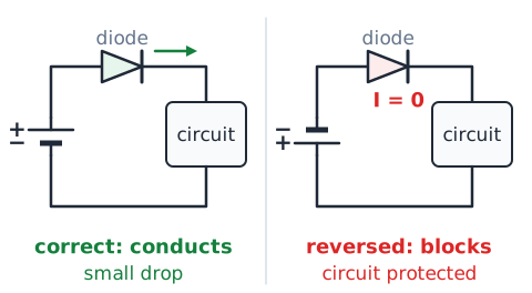
A diode is a two-terminal device built around one P–N junction. Its key feature is asymmetry: it conducts readily in one direction and blocks current in the other. A water-pipe check valve is a good comparison, since it lets water through one way and closes against backflow.
That one-way action is useful in many places: converting AC to DC, protecting a circuit when a battery is put in backward, steering signals, and absorbing voltage spikes. A diode does not store energy and does not create energy. It simply decides, based on polarity, whether current may pass.
Anode and cathode: learn the correct direction
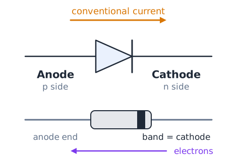
The diode's p side is the anode and its n side is the cathode. In the schematic symbol, the triangle is on the anode side and points toward a bar, which is the cathode. On the part itself, a printed band marks the cathode end.
Conventional current, which treats current as flowing from positive to negative, passes through a forward-biased diode from anode to cathode, the way the triangle points. Electrons move the opposite way, from cathode to anode. Keep the two descriptions separate: exam questions almost always use conventional current unless they say electron flow.
Forward bias reduces the junction barrier
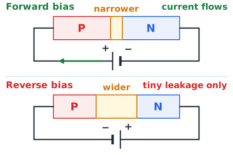
A diode is forward biased when its anode is made more positive than its cathode. The external voltage pushes holes in the p side and electrons in the n side toward the junction, which narrows the depletion region and lowers the barrier.
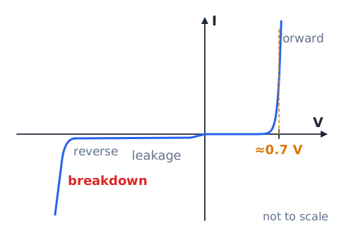
Once the applied voltage exceeds about 0.6 to 0.7 V for a silicon diode, current rises quickly. Above this point, the diode's voltage stays fairly steady while current is mostly set by the rest of the circuit. That is why a series resistor or some other limit is needed; a forward-biased diode on its own offers very little opposition to large currents.
Reverse bias raises the junction barrier
A diode is reverse biased when its cathode is made more positive than its anode. The external voltage pulls majority carriers away from the junction, widening the depletion region and raising the barrier.
Only a tiny leakage current flows, often in the microamp range or smaller, so for most purposes the diode is treated as off. This holds until the reverse voltage reaches the breakdown level. At breakdown, current rises sharply. Ordinary diodes can be damaged if pushed into breakdown with too much power, while Zener diodes are designed to operate there. Reverse bias does not remove the depletion region; it enlarges it.
Ideal diode versus physical diode
Exam problems use simplified diode models. The ideal model treats a diode as a perfect switch: zero voltage drop when forward biased and zero current when reverse biased. A slightly better model adds a fixed forward drop, often 0.7 V for silicon, 0.3 V for germanium, or around 2 V for a red LED.
Real diodes are more complicated. The forward drop changes with current and temperature, reverse leakage is small but not zero, and every part has maximum ratings. When a question gives a model value, use it exactly, and remember it is a convenient approximation, not a law.
Read diode polarity in a source–load loop
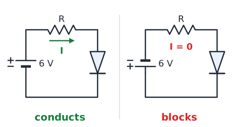
To decide whether a diode in a loop conducts, trace from the source's positive terminal. If you reach the diode's anode first and its cathode connects onward toward the negative terminal, the diode is forward biased and current flows, limited by the rest of the loop.
If you meet the cathode first, the diode is reverse biased and blocks current in that loop. Picture a simple circuit: a 6 V battery, a resistor, and a diode with its bar facing the negative terminal. That diode conducts. Flip the battery around and the same diode blocks, so the resistor carries essentially no current.
Rectification: change an AC waveform into one-polarity output
Rectification is the process of turning alternating current, which reverses direction many times per second, into current that flows in only one direction. In the US, household power completes 60 full cycles per second (60 Hz), while batteries and most electronics need one fixed polarity.
Diodes perform rectification by passing current only during the part of each cycle when they are forward biased. The output of a rectifier alone is not smooth DC; it is a series of one-polarity pulses. Further stages, such as filter capacitors and voltage regulators, smooth and steady the output into usable DC for a power supply.
Half-wave rectifier behavior
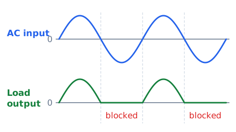
The simplest rectifier uses one diode in series with a load across an AC source. During the half of each cycle when the diode's anode is positive, it conducts and the load sees a positive hump. During the other half, the diode is reverse biased, blocks, and the load voltage is zero.
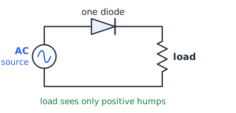
The result is a half-wave output: one hump, a flat gap, another hump, and so on. Only half of the input cycle is used, so this circuit wastes much of the available energy and has large gaps that are hard to smooth. It is still useful for simple, low-power jobs.
Full-wave bridge: the output current direction
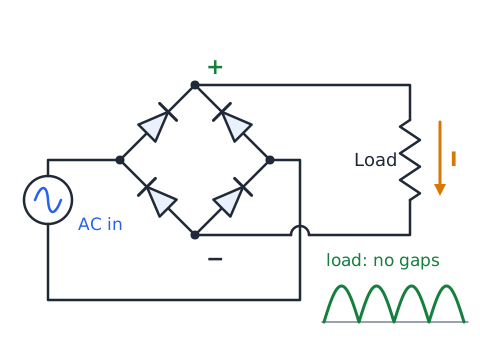
A bridge rectifier uses four diodes arranged in a diamond. On one half-cycle, two of the diodes conduct and steer current through the load in a given direction. On the next half-cycle, the other two conduct, and they steer current through the load in that same direction.
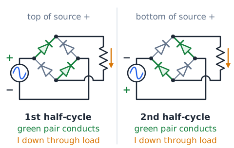
So both halves of the AC input produce output pulses with the same polarity. The output is a series of humps with no gaps between them, at twice the input frequency. Compared with half-wave rectification, it uses the whole input cycle and is easier to filter into smooth DC. Each path passes through two diode drops.
LEDs convert electrical energy into light
A light-emitting diode (LED) is a diode made from compound semiconductor materials, such as gallium arsenide or gallium nitride, rather than plain silicon. When it is forward biased, electrons cross the junction and drop into holes. In these materials, the energy given up comes out as light.
The color depends on the material and its band gap: red LEDs drop roughly 1.8 to 2.2 V, while blue and white LEDs drop about 3 V or more. LEDs are efficient, long-lasting, and switch on instantly, so they are used for indicators, displays, lighting, and remote controls (infrared). Like any diode, they light only when forward biased.
Why an LED needs current control
An LED's current rises very steeply once its forward voltage is reached. If you connect a 3 V LED straight to a 9 V battery, nothing in the loop limits the current, so it climbs far past the LED's rating and the device overheats and fails, sometimes in a flash.
The usual solution is a resistor in series. The resistor takes the extra voltage and sets the current, typically 10 to 20 mA for a small indicator LED. Brightness depends on current, not on voltage alone. Larger lighting LEDs often use a dedicated constant-current driver circuit instead of a simple resistor.
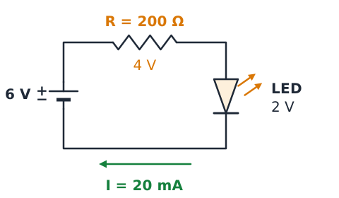
Compute a simple LED resistor
To size a series resistor for an LED, subtract the LED's forward drop from the supply voltage, then divide by the desired current:
is the supply voltage in volts, is the LED drop in volts, and I is the current in amperes. Example: a 6 V supply, a 2 V LED, and 20 mA give 4 V divided by 0.02 A, or 200 Ω.
Photodiode and light sensor distinction
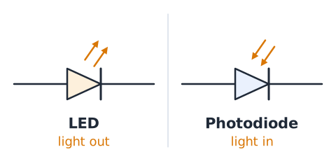
An LED and a photodiode are mirror images in purpose. The LED is an output device: electrical energy in, light out. A photodiode is an input or sensing device: light in, electrical response out.
A photodiode is usually operated reverse biased. When light strikes its junction, the light energy frees electrons and holes, and a small current flows that grows with the light level. That current can be measured to detect light, as in smoke detectors, TV remote receivers, light meters, and fiber-optic receivers. Solar cells work on the same idea but are designed to deliver power. In symbols, LED arrows point out, and photodiode arrows point in.
Zener diodes: reverse breakdown as a function
A Zener diode is designed to operate in reverse breakdown without damage. In the forward direction it behaves like an ordinary diode. In reverse, it blocks until the voltage reaches its rated Zener voltage, such as 5.1 V or 12 V, and then it conducts while keeping the voltage across it nearly constant.
This makes the Zener useful as a simple voltage reference or clamp: it holds a node at its rated voltage over a range of currents. It always needs a series resistor to limit current. Its symbol is a diode whose cathode bar has small bent ends, and it is installed with the cathode toward the positive side.
Zener clamp reasoning in an idealized model
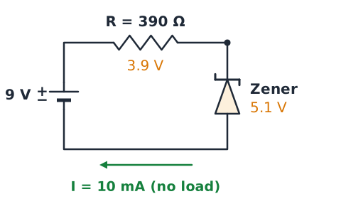
In the simple Zener model, the Zener holds its node at , so the series resistor carries the rest of the supply voltage:
That current splits between the Zener and any load:
Example: a 9 V source, a 5.1 V Zener, and 390 Ω give 3.9 V divided by 390 Ω, or 10 mA. With no load, all 10 mA flows through the Zener.
Transistors: switch and signal amplifier
A transistor is a three-terminal semiconductor device in which a small signal at one terminal controls a larger current between the other two. That gives it two main jobs.
As a switch, the transistor is driven either fully on or fully off, so a weak control signal, such as from a microcontroller pin, can turn on a motor, a relay, or a lamp. As an amplifier, it is held partway on, so small changes at the input produce larger copies at the output, as in an audio amplifier. The transistor does not create energy; the power comes from the supply.
BJT terminal names and the arrow clue
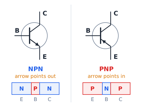
A bipolar junction transistor (BJT) has three layers of doped silicon and three terminals: emitter, base, and collector. In an NPN transistor, a thin p-type base sits between n-type emitter and collector; a PNP transistor has the opposite pattern.
In the schematic symbol, the emitter lead carries an arrow showing the direction of conventional current through the base-emitter junction. If the arrow points out, away from the base, the transistor is NPN. If it points in, toward the base, it is PNP. The base is the control terminal, and the collector usually connects toward the load.
NPN switching as an ideal model
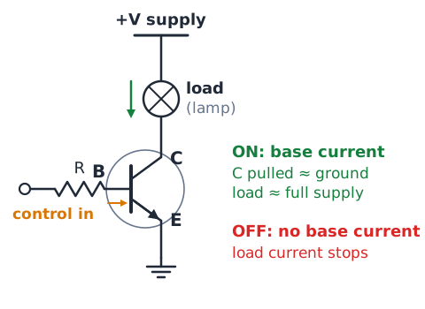
A common way to use an NPN transistor as a switch is the low-side arrangement. The load, such as a lamp or relay coil, connects between the positive supply and the collector. The emitter goes to ground. A control voltage feeds the base through a resistor.
When the base gets enough current, the transistor turns on and the collector is pulled close to ground, so the load gets nearly the full supply voltage. When the base current is removed, the transistor turns off and the load current stops. In this ideal model the transistor acts like a switch on the ground side of the load.
BJT active, cutoff and saturation
A BJT operates in one of three main regions. In cutoff, the base-emitter junction is not forward biased, essentially no collector current flows, and the transistor is off.
In the active region, the base-emitter junction is forward biased and the collector current is roughly proportional to the base current. This is the amplifier region. In saturation, the base current is more than enough, the collector current is limited by the outside circuit rather than the transistor, and the collector-emitter voltage is very small, often 0.2 V or so. A switch alternates between cutoff and saturation.
Current gain is a ratio, not a source
In the active region, a BJT's collector current is a multiple of its base current. That multiple is the DC current gain, called beta () or :
Beta is a ratio, so it has no units. It does not mean the transistor creates current from nothing; the collector current comes from the power supply, and the base current only controls it. The emitter carries both:
Typical small transistors have beta values from about 50 to 300.
Compute transistor gain correctly
To find beta, divide collector current by base current, using the same unit for both. Example: a transistor carries 72 mA at the collector with 0.9 mA at the base.
The emitter current is 72.9 mA. Common mistakes are dividing upside down, which would give 0.0125, and subtracting instead of dividing.
Field-effect transistor basic control
A field-effect transistor (FET) controls current with an electric field instead of a base current. Its terminals are the gate, the drain, and the source. Current flows through a channel between the drain and source, and the voltage between the gate and the source controls how well that channel conducts.
In a MOSFET, the most common type, the gate is separated from the channel by a very thin insulating layer of oxide. So in steady operation, almost no current flows into the gate. That makes MOSFETs easy to drive from logic circuits and very popular as power switches.
MOSFET switching and gate thresholds
For an enhancement-mode n-channel MOSFET, the channel is off when the gate-to-source voltage () is zero. As rises past the threshold voltage, a channel begins to form and a small current flows.
The threshold is only the point where conduction starts, usually measured at a very small test current. To switch a large load with low resistance, the gate must be driven well above threshold, to a value the datasheet lists for its specified on-resistance. Once the gate is charged, holding it on takes almost no current, but charging and discharging the gate quickly takes brief pulses of current.
BJT versus MOSFET comparison
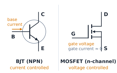
A BJT is current controlled: you must supply a steady base current to keep it on. A MOSFET is voltage controlled: once the gate is charged to the right voltage, almost no gate current is needed.
BJT terminals are emitter, base, and collector; MOSFET terminals are source, gate, and drain. Both can switch and amplify. A saturated BJT has a fairly fixed small voltage drop, while an on MOSFET acts more like a small resistance, which can be very low in power devices. BJTs are common in simple analog circuits, and MOSFETs dominate digital chips and many power switches.
Integrated circuits put many devices together
An integrated circuit (IC), or chip, combines many transistors, diodes, resistors, and sometimes capacitors on one small piece of silicon, all wired together during manufacturing. A simple IC may hold a few dozen parts; a modern processor holds billions of transistors.
Packing parts together saves space, lowers cost, uses less power, and improves reliability, since there are fewer separate connections. ICs come in packages with rows of pins and are labeled U or IC on schematics. Common examples include timers, voltage regulators, operational amplifiers, logic gates, memory, and microprocessors.
Logic gates turn input states into outputs
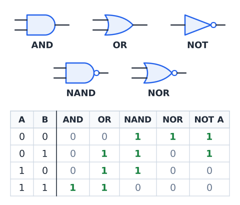
Digital circuits use voltage levels to stand for two states, often called 1 (high) and 0 (low). Logic gates, built from transistors inside ICs, produce an output based on the states of their inputs.
An AND gate outputs 1 only if all inputs are 1. An OR gate outputs 1 if any input is 1. A NOT gate, or inverter, flips its single input. NAND and NOR are AND and OR followed by an inverter. For example, an alarm that sounds only when a door is open and the system is armed is AND logic.
Rectifier, regulator, amplifier: separate jobs
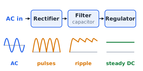
Power supplies and audio systems use several stages, and each has its own job. A rectifier changes AC into one-direction pulses. A filter, usually a large capacitor, smooths those pulses into a fairly steady voltage with some ripple.
A regulator, which might be a Zener diode circuit or a regulator IC, holds the output at a set voltage even as the input or the load changes. An amplifier, built around transistors, makes a weak signal larger using power from the supply. Questions may describe a function and ask for the device; match the job, not just a familiar name.
Reverse-polarity protection
Many battery-powered devices can be damaged if the battery is inserted backward. A simple protection is a diode in series with the positive supply line, with its anode toward the battery's positive terminal.
With correct polarity, the diode is forward biased and the circuit works, minus a small voltage drop. With reversed polarity, the diode is reverse biased and blocks current, protecting the circuit. The cost is the diode's forward drop and the heat it causes. Designers who cannot spare that drop often use a MOSFET arranged to do the same job with less loss.
Flyback diodes in inductive switching
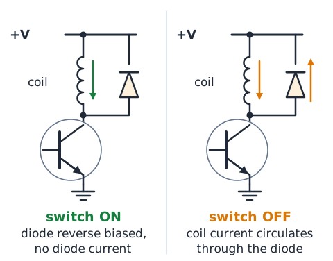
Coils such as relay windings and motor windings resist sudden changes in current. When a transistor switch suddenly turns off the current to a coil, the collapsing magnetic field produces a large voltage spike that can destroy the transistor.
A flyback diode, also called a freewheeling or snubber diode, is placed across the coil to prevent this. It is installed reverse biased during normal operation: cathode toward the positive supply, anode toward the transistor. When the switch opens, the coil's voltage reverses, the diode becomes forward biased, and it gives the coil current a safe loop to die away in.
Battery versus semiconductor energy source
A battery is a source: it converts chemical energy into electrical energy and pushes current around a circuit. Diodes, transistors, and ICs are not sources. They control, steer, or convert energy that some source provides.
A transistor amplifier's larger output comes from the power supply, not from the transistor. An LED's light comes from the energy delivered by the supply. Even a photodiode or solar cell is better described as converting light energy, not creating energy. If a question offers an answer such as "the transistor provides power without a supply," eliminate it, because no device makes energy from nothing.
How semiconductor switching differs from mechanical relays
A relay switches a load using a coil that moves physical metal contacts. A transistor switches using semiconductor material with no moving parts.
Transistors switch much faster, often millions of times per second, do not wear out from contact arcing, make no click, and need little control power. Relays offer complete electrical isolation between the control circuit and the load, can handle AC or DC in either direction, and have very low resistance when closed. Relays are also more tolerant of brief overloads. Many systems combine them: a transistor drives the relay coil, and the relay switches the heavy load.
Use a safe troubleshooting logic sequence
When an electronic circuit fails, follow a careful sequence. First, make sure the power is off and capacitors are discharged before touching parts. Second, look for obvious signs: burned resistors, swollen capacitors, cracked parts, or loose connections.
Third, check the power source and fuses. Fourth, with power applied and proper care, measure voltages at key points and compare them with expected values. Fifth, with power removed, test suspect parts using resistance or diode-test functions. Change one thing at a time and recheck. Replace a failed part with an equal rating, and find the cause, such as a short or overheating, before restoring power.
Diode-test interpretation is conditional
Many multimeters have a diode-test setting that pushes a small current through a part and shows the resulting voltage. A good silicon diode usually reads about 0.5 to 0.7 V in the forward direction and shows open (often "OL") in reverse.
These results are only meaningful under the right conditions: power off, and ideally the diode removed from the circuit, because other parts in parallel can change the reading. A reading of near zero both ways suggests a shorted diode; open both ways suggests an open diode. LEDs may need a higher test voltage than some meters provide, so a dark LED in diode test is not proof of failure.
Thermal and current ratings protect components
Every semiconductor device has limits listed on its datasheet: maximum current, maximum voltage, maximum power, and maximum temperature. Exceeding them, even briefly in some cases, can destroy the part.
Power turns into heat, and heat is the main enemy. A diode carrying 2 A with a 1 V drop dissipates 2 W, which is enough to need a heat sink in many packages. Designers keep a safety margin, use heat sinks and airflow, and add fuses or current limits. Hot semiconductors also change behavior, often conducting more as they warm, which can lead to runaway heating if not controlled.
Conventional-current and electron-direction traps
Two current-direction conventions exist. Conventional current is defined as flowing from the positive terminal through the circuit to the negative terminal. Electron flow describes the actual motion of electrons, from negative to positive.
Both describe the same circuit correctly; they are just opposite in direction. Semiconductor symbols are drawn for conventional current: the diode triangle and the transistor emitter arrow point the way conventional current flows. If a question uses electron flow, the electrons move against those arrows. Read the stem carefully, and do not switch conventions partway through a problem.
What rectification does not promise
A rectifier's output flows in only one direction, but that does not make it smooth, constant, or regulated. Without a filter, it is a series of pulses that rise and fall with the AC input.
Adding a capacitor smooths the pulses but leaves some ripple, which grows as the load draws more current. A regulator is needed to hold the output steady when the input or load changes. A rectifier also does not change the input frequency to zero or create power. It only redirects current so that it always passes through the load in the same direction.
Choose the correct device from a functional description
Exam stems often describe a job and ask which device does it. Match the function. One-way conduction or AC-to-DC conversion: rectifier diode. Light output: LED. Light sensing: photodiode. Holding a steady reference voltage using reverse breakdown: Zener diode.
Switching a load or amplifying a signal: transistor (BJT or MOSFET). Many devices combined in one package: integrated circuit. Absorbing a coil's turn-off spike: flyback diode. Storing charge: capacitor, which is not a semiconductor junction device. Decide the job first, then pick the device.
Recognize the difference between PN and transistor structure
A diode has one P–N junction and two terminals: anode and cathode. A bipolar transistor has two junctions sharing a thin middle layer, giving three terminals: emitter, base, and collector. NPN means n-type emitter, p-type base, and n-type collector.
The thin base is what makes transistor action possible; two separate diodes wired back to back cannot amplify. A MOSFET uses a different idea: an insulated gate controls a channel between source and drain. When a question asks how many layers, junctions, or terminals a device has, use this structure.
Dimensional checks for electronic examples
Checking units catches many errors. Volts divided by ohms gives amperes, volts times amperes gives watts, and watts times seconds gives joules:
Beta is milliamps divided by milliamps, so it has no unit. Convert prefixes first: 20 mA is 0.02 A and 4.7 kΩ is 4,700 Ω. If an LED resistor answer comes out in watts, or a current comes out in ohms, a formula was set up wrong.
Read specifications as conditions rather than universal constants
Values on a datasheet are measured under stated conditions, such as a certain current, temperature, or test voltage. A diode's forward drop of 0.7 V, a transistor's beta of 100, or a MOSFET's threshold of 2 V are not fixed constants for every situation.
Forward drop rises with current and falls as temperature rises. Beta varies from one transistor to the next of the same type and changes with current and temperature. On an exam, use the value given, but recognize answer choices that treat a model number as universal. Good designs work across the whole range of a device's possible values.
Exam technique for symbols and device behavior
For semiconductor questions, read the symbol details first: triangle and bar for diodes, arrow direction for LEDs and photodiodes and NPN or PNP, bent bar tips for Zener diodes, gate, drain, and source for MOSFETs.
Then decide polarity: which terminal is more positive? That tells you forward or reverse bias. For calculations, write down the given model values and subtract any fixed drops before applying Ohm's law. Check units and magnitude. Finally, eliminate impossible choices, such as devices that create energy, diodes that conduct equally both ways, or currents that ignore the limits of the outside circuit.
Example 1 — Identify donor doping
Problem: A small amount of phosphorus, which has five valence electrons, is added to pure silicon. What type of material forms, and what is the majority carrier?
Step 1: Silicon has four valence electrons. Step 2: Phosphorus has one extra electron that is loosely bound. Step 3: Atoms that give away electrons are donors.
Answer: N-type silicon, with free electrons as the majority carriers.
Example 2 — Identify acceptor doping
Problem: Boron, with three valence electrons, is added to silicon. What forms?
Step 1: Boron can complete only three of four bonds. Step 2: The missing electron leaves a hole, so boron is an acceptor.
Answer: P-type silicon, with holes as the majority carriers and electrons as minority carriers.
Example 3 — Find diode bias
Problem: A diode has its anode connected to a node at 3 V and its cathode connected to a node at 8 V. Is it forward or reverse biased, and does it conduct in the normal model?
Step 1: Compare: the cathode is 5 V more positive than the anode. Step 2: Cathode more positive means reverse bias.
Answer: Reverse biased. Only a tiny leakage current flows, assuming 5 V is below its breakdown voltage.
Example 4 — Supply minus diode drop
Problem: A 9 V source, a silicon diode modeled at 0.7 V, and a 1 kΩ resistor are in series. Find the current.
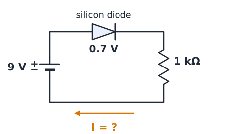
Step 1: The resistor gets 9 V minus 0.7 V, which is 8.3 V.
Answer: 8.3 mA.
Example 5 — LED resistor with 12 V source
Problem: A white LED modeled at 3.2 V must run at 20 mA from a 12 V supply. Find the resistor.
Step 1: The resistor gets 12 V minus 3.2 V, which is 8.8 V.
Answer: 440 Ω.
Example 6 — LED resistor power
Problem: The 440 Ω resistor from the previous example carries 20 mA. How much power does it dissipate, and is a 1/4 W part enough?
Answer: 0.176 W. A 0.25 W resistor works, with some margin.
Example 7 — Recognize a half-wave output
Problem: An oscilloscope across a load shows a positive hump lasting half a cycle, then a flat line at zero for the next half cycle, repeating. The input is a sine wave. What circuit produced this?
Step 1: Only one polarity appears. Step 2: Every other half-cycle is missing, not flipped.
Answer: A half-wave rectifier with a single diode; the diode blocks during the missing half-cycles.
Example 8 — Identify a bridge rectifier
Problem: A power supply has four diodes in a diamond between a transformer and a load. The load shows positive humps with no gaps, at twice the AC frequency. Identify the circuit.
Step 1: Four diodes in a diamond is the bridge layout. Step 2: No gaps means both half-cycles are used.
Answer: A full-wave bridge rectifier.
Example 9 — Compute Zener series current
Problem: An 18 V source feeds a 12 V Zener through 200 Ω. A load across the Zener draws 10 mA. Find the resistor and Zener currents.
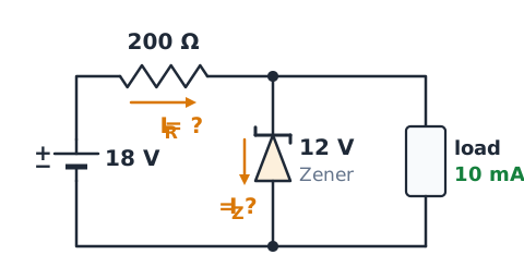
Then the Zener takes the rest: 30 mA minus 10 mA.
Answer: 30 mA in the resistor and 20 mA in the Zener.
Example 10 — Calculate BJT current gain
Problem: A transistor in the active region has a base current of 0.2 mA and a collector current of 24 mA. Find beta.
Answer: Beta is 120, with no units. The emitter carries 24.2 mA.
Example 11 — Predict collector current conditionally
Problem: A transistor with beta 100 gets 0.3 mA of base current. Its load is 500 Ω on a 5 V supply. Find the collector current.
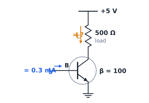
Step 1: Beta predicts 30 mA. Step 2: The load allows at most 5 V divided by 500 Ω, or 10 mA.
Answer: About 10 mA. The transistor saturates; the outside circuit sets the limit.
Example 12 — MOSFET control classification
Problem: A device has terminals labeled G, D, and S. Raising the G-to-S voltage from 0 V to 10 V lets a lamp between the supply and D light, and almost no current enters G. Classify it.
Step 1: Gate, drain, and source are FET terminals. Step 2: Control by voltage with almost no gate current fits an insulated gate.
Answer: An n-channel enhancement MOSFET used as a switch.
Example 13 — Estimate a diode loss
Problem: A rectifier diode carries a steady 1.5 A with a stated 0.9 V forward drop. Find its power loss and the heat produced in one minute.
Answer: 1.35 W and 81 J.
Example 14 — Choose a flyback path
Problem: A 24 V relay coil is switched on its low side by an NPN transistor. How should the flyback diode be connected?
Step 1: While energized, the top of the coil is at +24 V, so the diode must be reverse biased then. Step 2: Put the cathode at the +24 V end and the anode at the collector end.
Answer: Cathode to supply, anode to transistor. At turn-off, the spike forward biases the diode, and coil current circulates safely through it.
Drill 1 — Carrier classification
Prompt: Arsenic doping gives which type? Answer: N-type, majority electrons.
Prompt: Gallium doping gives which type? Answer: P-type, majority holes.
Prompt: Minority carriers in n-type silicon? Answer: Holes.
Prompt: Is p-type silicon positively charged overall? Answer: No, it is neutral.
Drill 2 — One-way conduction
Prompt: Anode at 5 V, cathode at 0 V. Conducts? Answer: Yes, forward biased.
Prompt: Anode at 0 V, cathode at 5 V, Zener rating 12 V. Conducts? Answer: No, reverse biased below breakdown.
Prompt: Which way does conventional current pass? Answer: Anode to cathode.
Drill 3 — LED calculation
Prompt: 5 V supply, 1.8 V LED, 16 mA. Resistor? Answer: 3.2 V divided by 0.016 A, or 200 Ω.
Prompt: 9 V supply, 2 V LED, 10 mA. Resistor? Answer: 7 V divided by 0.01 A, or 700 Ω.
Drill 4 — Assign electronic functions
Prompt: Device that holds a 5.1 V reference? Answer: Zener diode.
Prompt: Converts AC to one-direction pulses? Answer: Rectifier.
Prompt: Senses light? Answer: Photodiode.
Prompt: Lets a logic pin switch a motor? Answer: Transistor.
Prompt: Thousands of parts on one chip? Answer: Integrated circuit.
Drill 5 — BJT current gain
Prompt: Collector 40 mA, base 0.5 mA. Beta? Answer: 80.
Prompt: Beta 200, base 0.05 mA. Collector current if the circuit allows it? Answer: 10 mA.
Drill 6 — Failure reasoning
Prompt: An LED wired straight to a 9 V battery burns out. Why? Answer: No series resistor limited its current.
Prompt: A transistor driving a relay coil fails repeatedly. What is missing? Answer: A flyback diode across the coil.
Prompt: A battery went in backward and a series diode was fitted. Damage? Answer: None; the diode blocked.
ASVAB reasoning sequence
Use a steady sequence on semiconductor questions. First, name the device from its symbol or function. Second, decide the polarity at its terminals and whether it is forward biased, reverse biased, on, or off.
Third, list given values: supply voltage, model drops, resistances, currents, beta. Fourth, subtract fixed drops, then apply Ohm's law or the power formula, converting milli to base units. Fifth, check limits: a transistor cannot carry more current than its load allows, and a diode drop is a model value. Finally, reject choices where energy appears from nowhere.
Nine high-impact misconceptions
First: n-type is negatively charged. In fact both n and p material are neutral; the letters name the majority carrier.
Second: current flows cathode to anode. Conventional current flows anode to cathode.
Third: reverse bias erases the depletion region. It widens it.
Fourth: a diode always drops exactly 0.7 V. That is only a model value.
Fifth: LEDs can go straight across a battery. They need current limiting.
Sixth: a rectifier gives smooth DC. It gives pulses until filtered and regulated.
Seventh: beta creates current. The supply provides it; beta is a ratio.
Eighth: beta times base current is always the collector current. Saturation limits it.
Ninth: reaching the MOSFET threshold means fully on. It only begins conducting.
Premium review: devices, units and assumptions
Silicon becomes useful when doped: donors with five valence electrons make n-type material with electron majority carriers, and acceptors with three make p-type material with hole majority carriers. A P–N junction forms a diode that conducts from anode to cathode when forward biased and blocks when reverse biased until breakdown.
LEDs emit light, photodiodes sense light, and Zener diodes hold a reference voltage in reverse breakdown. Half-wave rectifiers use one half-cycle; bridges use both. BJTs (emitter, base, collector) are current controlled with
MOSFETs (gate, drain, source) are voltage controlled.
Key formulas: LED resistor equals supply minus LED drop, divided by current; power equals voltage times current. Always treat given drops and gains as model values.
 English ▾